
鲍哲南院士柔性电子最新突破-高速和大规模本征可拉伸集成电路
研究背景
与人体无缝结合的类肤电子设备将实现舒适、大规模和高保真的生理监测、健康状况实时分析、局部治疗、用于假肢的传感器运动功能重建和增强现实。为了实现器件的适形性和拉伸能力,人们研究了三种不同的方法:(1)结构工程,如屈曲、褶皱或剪纸(kirigami)结构;(2)与可拉伸导体相互连接的有源元件的刚度工程;(3)本征可拉伸电子学。其中,本征可拉伸电子学具有独特的优势,即使在运动和尺寸变化的情况下也能与组织亲密接触,因此是人机界面、可穿戴和植入式的理想平台。
为实现先进的类肤电子器件所需的传感、处理和驱动功能,需要高性能本征可拉伸晶体管和大规模集成电路(图 1a)。为此,人们通过材料创新和器件工程为开发可拉伸电子器件做出了巨大努力。在实现高空间分辨率和电气性能方面仍然存在挑战。虽然最近在材料设计方面的尝试使导体、半导体和电介质层可直接进行光图案化,并提高了器件密度但可拉伸器件的电气性能仍比大多数柔性薄膜器件低几个数量级,特别是在短沟道长度时(例如,按沟道宽度归一化的半导体载流子迁移率和高金属-半导体导通电阻。在电路层面,迄今为止使用本征可拉伸材料实现的最大集成度为 54 个晶体管和 14 个逻辑门。此外,据我们所知,目前报道的最高运行速度仅为 330 Hz,远远低于实际应用的要求(例如,用于显示驱动、信号调节或生理监测的速度大于 10kHz)。因此,目前的类肤电子器件只能实现一些基本功能,如通过有限的输出端子进行慢速信号处理。
研究成果
具有类肤机械特性的本征可拉伸电子器件已被认为是一种前景广阔的新兴应用平台,其应用范围从连续生理监测到健康状况实时分析,再到自主医疗的闭环传输。然而,目前的技术只能达到非晶硅水平的电气性能(即电荷载流子迁移率约为1cm2 V-1 s-1),集成度低(例如,每个电路只有 54 个晶体管),功能有限。在此,鲍哲南院士团队报告了具有高驱动能力、高运行速度和大规模集成的高密度本征可拉伸晶体管和集成电路。材料、制造工艺设计、器件工程和电路设计等方面的创新使它们得以实现。该本征可拉伸晶体管在100%应变条件下的平均场效应迁移率超过 20 cm2V-1s-1,器件密度为每平方厘米 100000 个晶体管(包括互连器件),在5 V电源电压下的高驱动电流约为2 uA μm-1。值得注意的是,这些参数与塑料基底上基于金属氧化物、碳纳米管和多晶硅材料的最先进可熔晶体管不相上下。此外,据我们所知,在本征可拉伸电子器件中,首次实现了拥有 1000 多个晶体管、阶段开关频率超过1 MHz 的大规模集成电路。此外,还展示了一种高通量盲文识别系统,它超越了人类皮肤的感应能力,该系统由一个有源矩阵触觉传感器阵列(密度达到创纪录的每平方厘米 2500 个单元)和一个发光二极管显示屏(刷新速度高达60 Hz,且具有出色的机械坚固性)实现。上述设备性能的进步大大提高了类肤电子设备的能力。相关研究以“High-speed and large-scale intrinsically stretchable integrated circuits”为题发表在Nature期刊上。
图文导读
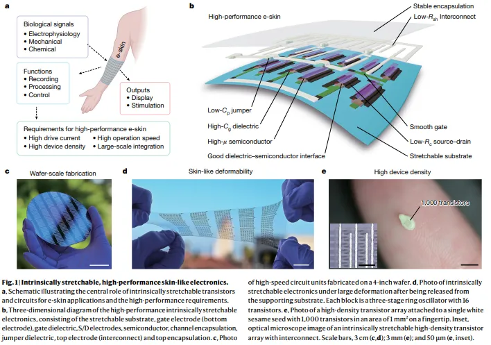
Fig. 1 | Intrinsically stretchable, high-performance skin-like electronics. a, Schematic illustrating the central role of intrinsically stretchable transistors and circuits for e-skin applications and the high-performance requirements. b, Three-dimensional diagram of the high-performance intrinsically stretchable electronics, consisting of the stretchable substrate, gate electrode (bottom electrode), gate dielectric, S/D electrodes, semiconductor, channel encapsulation, jumper dielectric, top electrode (interconnect) and top encapsulation. c, Photo of high-speed circuit units fabricated on a 4-inch wafer. d, Photo of intrinsically stretchable electronics under large deformation after being released from the supporting substrate. Each block is a three-stage ring oscillator with 16 transistors. e, Photo of a high-density transistor array attached to a single white sesame seed with 1,000 transistors in an area of 1 mm2 on a fingertip. Inset, optical microscope image of an intrinsically stretchable high-density transistor array with interconnect. Scale bars, 3 cm (c,d); 3 mm (e); and 50 μm (e, inset).
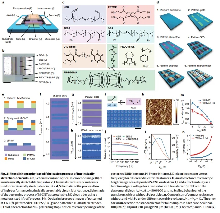
Fig. 2 | Photolithography-based fabrication process of intrinsically stretchable circuits. a,b, Schematic (a) and optical microscope image (b) of an intrinsically stretchable transistor. c, Chemical structures of materials used for intrinsically stretchable circuits. d, Schematic of the process flow of high-performance intrinsically stretchable circuit fabrication. e, Schematic of the patterning process of M-CNT as stretchable S/D electrodes using a metal-assisted lift-off process. f–h, Optical microscope images of patterned M-CNT (f), patterned PEDOT:PSS/PR (g) and patterned EGaIn (h) electrodes. i, Thiol-ene reaction for NBR patterning (top), optical microscope image of the patterned NBR (bottom). Pi, Photo-initiator. j, Dielectric constant versus frequency for different dielectric elastomers. k, An atomic force microscope height image of as-deposited S-CNT on dextran. l, Field-effect mobility as a function of gate voltage for a transistor with transferred S-CNT onto the elastomer dielectric. Wch /Lch = 800/100 μm. m, Scaling behaviour of the transistors with or without Pd particles. n, Comparison of contact resistance without and with Pd under different overdrive voltages. VOV = Vgs – Vth . The error bars in m describe the standard error for four samples in each case. Scale bar, 100 μm (b); 10 μm (f); 10 μm (g); 20 μm (h); 40 μm (i, bottom); and 500 nm (k).
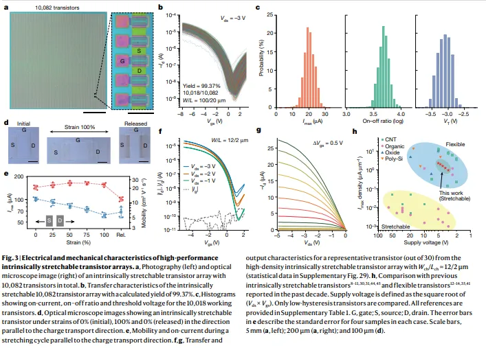
Fig. 3 | Electrical and mechanical characteristics of high-performance intrinsically stretchable transistor arrays. a, Photography (left) and optical microscope image (right) of an intrinsically stretchable transistor array with 10,082 transistors in total. b, Transfer characteristics of the intrinsically stretchable 10,082 transistor array with a calculated yield of 99.37%. c, Histograms showing on-current, on–off ratio and threshold voltage for the 10,018 working transistors. d, Optical microscope images showing an intrinsically stretchable transistor under strains of 0% (initial), 100% and 0% (released) in the direction parallel to the charge transport direction. e, Mobility and on-current during a stretching cycle parallel to the charge transport direction. f,g, Transfer and output characteristics for a representative transistor (out of 30) from the high-density intrinsically stretchable transistor array with Wch /Lch ≈ 12/2 μm (statistical data in Supplementary Fig. 29). h, Comparison with previous intrinsically stretchable transistors8–11,30,31,44,45 and flexible transistors12–14,35,41 reported in the past decade. Supply voltage is defined as the square root of (Vds × Vgs ). Only low-hysteresis transistors are compared. All references are provided in Supplementary Table 1. G, gate; S, source; D, drain. The error bars in e describe the standard error for four samples in each case. Scale bars, 5 mm (a, left); 200 μm (a, right); and 100 μm (d).
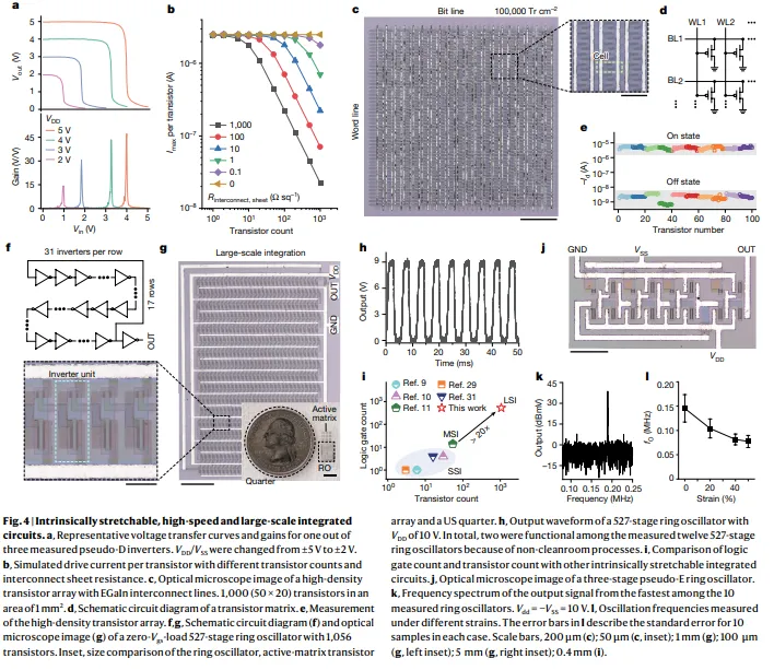
Fig. 4 | Intrinsically stretchable, high-speed and large-scale integrated circuits. a, Representative voltage transfer curves and gains for one out of three measured pseudo-D inverters. VDD /VSS were changed from ±5 V to ±2 V. b, Simulated drive current per transistor with different transistor counts and interconnect sheet resistance. c, Optical microscope image of a high-density transistor array with EGaIn interconnect lines. 1,000 (50 × 20) transistors in an area of 1 mm2. d, Schematic circuit diagram of a transistor matrix. e, Measurement of the high-density transistor array. f,g, Schematic circuit diagram (f) and optical microscope image (g) of a zero-Vgs-load 527-stage ring oscillator with 1,056 transistors. Inset, size comparison of the ring oscillator, active-matrix transistor array and a US quarter. h, Output waveform of a 527-stage ring oscillator with VDD of 10 V. In total, two were functional among the measured twelve 527-stage ring oscillators because of non-cleanroom processes. i, Comparison of logic gate count and transistor count with other intrinsically stretchable integrated circuits. j, Optical microscope image of a three-stage pseudo-E ring oscillator. k, Frequency spectrum of the output signal from the fastest among the 10 measured ring oscillators. Vdd = −VSS = 10 V. l, Oscillation frequencies measured under different strains. The error bars in l describe the standard error for 10 samples in each case. Scale bars, 200 μm (c); 50 μm (c, inset); 1 mm (g); 100 μm (g, left inset); 5 mm (g, right inset); 0.4 mm (i).
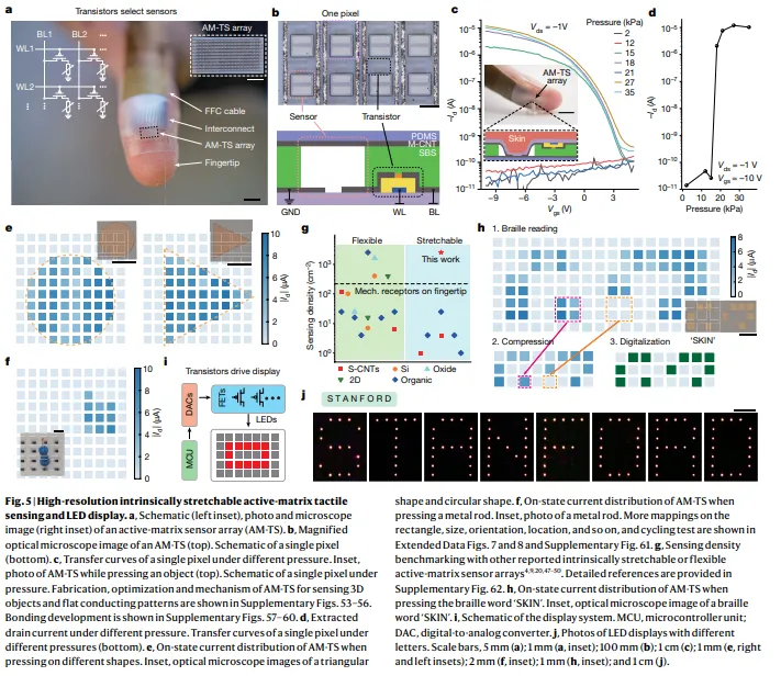
Fig. 5 | High-resolution intrinsically stretchable active-matrix tactile sensing and LED display. a, Schematic (left inset), photo and microscope image (right inset) of an active-matrix sensor array (AM-TS). b, Magnified optical microscope image of an AM-TS (top). Schematic of a single pixel (bottom). c, Transfer curves of a single pixel under different pressure. Inset, photo of AM-TS while pressing an object (top). Schematic of a single pixel under pressure. Fabrication, optimization and mechanism of AM-TS for sensing 3D objects and flat conducting patterns are shown in Supplementary Figs. 53–56. Bonding development is shown in Supplementary Figs. 57–60. d, Extracted drain current under different pressure. Transfer curves of a single pixel under different pressures (bottom). e, On-state current distribution of AM-TS when pressing on different shapes. Inset, optical microscope images of a triangular shape and circular shape. f, On-state current distribution of AM-TS when pressing a metal rod. Inset, photo of a metal rod. More mappings on the rectangle, size, orientation, location, and so on, and cycling test are shown in Extended Data Figs. 7 and 8 and Supplementary Fig. 61. g, Sensing density benchmarking with other reported intrinsically stretchable or flexible active-matrix sensor arrays4,9,20,47–50. Detailed references are provided in Supplementary Fig. 62. h, On-state current distribution of AM-TS when pressing the braille word ‘SKIN’. Inset, optical microscope image of a braille word ‘SKIN’. i, Schematic of the display system. MCU, microcontroller unit; DAC, digital-to-analog converter. j, Photos of LED displays with different letters. Scale bars, 5 mm (a); 1 mm (a, inset); 100 mm (b); 1 cm (c); 1 mm (e, right and left insets); 2 mm (f, inset); 1 mm (h, inset); and 1 cm (j).
总结与展望
总之,通过合理的材料设计与制备、加工和器件工程,作者实现了具有前所未有性能的本征可拉伸类肤集成电路的里程碑。据我们所知,实现了创纪录的高晶体管阵列密度、良好的机械稳健性、高产量和高驱动能力。具体地说,实现了拥有1000 多个晶体管的大规模本征可拉伸集成电路,并将分级开关频率推高至MHz级。通过合理选择材料、界面工程和工艺设计,最大限度地减少了晶体管沟道长度,同时降低了寄生电容和互连电阻,最后,利用本征可拉伸晶体管阵列演示了:(1)高分辨率盲文识别和小物体形状感应其能力超过了人类皮肤;(2)刷新率为60Hz的 LED 显示器,在变形情况下性能稳定。该高性能本征可拉伸电子器件是实现未来实际皮肤应用中各种功能的关键构件,例如高频率生理信号采集、本地放大器阵列、皮肤计算、显示和闭环驱动。
文献链接:
High-speed and large-scale intrinsically stretchable integrated circuits
https://www.nature.com/articles/s41586-024-07096-7